On October 14, 2026, GlobalFoundries (Nasdaq: GFS) announced that it was selected as technology provider and operator for two new 300mm semiconductor fabs at its Malta, New York site, under a US-Japan initiative of up to $21 billion that the company says is enabled by President Trump's trade and investment agreement with Japan. In a separate agreement, the US Department of Commerce will take an equity stake of about 4% in GF. This article sets out what the company and press coverage confirm, runs some simple arithmetic on the numbers, and lists what has not been disclosed, including the process node, which the announcement does not name.
What was announced
According to GlobalFoundries' release, Japan supplies the investment while GF contributes its technology, manufacturing expertise and operational capabilities. An initial investment of about $10 billion is meant to accelerate construction of the first fab, and a second fab of roughly the same cost follows. The first fab is expected to come online in 2029, and groundbreaking is planned for later in 2026 on a site the company describes as permitted and shovel-ready. The release gives no date for the second fab. It also cites about 27,000 construction and ecosystem jobs and more than 1,000 high-skilled manufacturing jobs in New York's Capital Region.
Commerce Secretary Howard Lutnick framed the deal as showing how the President's trade agreements result in "transformational American industrial assets." The release also carries supportive statements from Renesas, Tokyo Electron, Apple, Cirrus Logic and GM; whether these correspond to binding purchase commitments is not stated.
How the money and ownership work
Hoodline's report, which cites Reuters, adds details that the release does not. It says the two fabs will be jointly owned by the US government and Japanese interests, that GF CEO Tim Breen told Reuters the US government will own about 7% of GF in total once other agreements are counted, and that available free cash flow is split evenly between the US and Japan until an unstated threshold, after which 90% goes to the US. We could not open Reuters directly, so these points rest on that secondary account. The same report says President Trump selects which projects Japan funds, and traces the arrangement to Japan's 2025 pledge of $550 billion of US investment in exchange for lower US tariffs.
Two numbers do not reconcile publicly. The release says about 4%, the CEO is quoted as saying about 7% in total, and the difference of roughly 3 percentage points is attributed to "other agreements" that coverage does not identify. Neither the form of Japan's financing (loan, equity or other), the responsible Japanese entity, nor the free-cash-flow threshold is disclosed.
The announcement names the money, the capacity and the date. It does not name the process node, the financing instrument or the cash-flow threshold.
What the public record leaves open
The government equity pattern
A US equity stake in a chipmaker is not new. In August 2025 the US government agreed to buy 433.3 million Intel shares at $20.47 each, about a 9.9% stake for $8.9 billion, funded from $5.7 billion of unpaid CHIPS Act grants and $3.2 billion from the Secure Enclave program, according to Manufacturing Dive. The government's role was described as passive, with no board seats, plus a warrant for an additional 5% if Intel's ownership of its foundry business fell below 51% within five years. We covered Intel's later capital raise in Intel's $15 billion stock offering.
The two cases differ in structure. At Intel the stake was a conversion of grants already awarded. At GF the 4% stake is described as a separate agreement from the amended CHIPS award, and the capital for the new fabs comes from Japan, not from the US Treasury. That makes the Malta deal closer to a three-party model: foreign capital, US ownership participation and an incumbent operator.
Reading the wafer numbers
The release says each fab adds about 900,000 300mm wafers of annual US capacity at full operation. The unit is 300mm (12-inch) wafers per year. The release does not say whether this counts wafer starts or finished wafers, or which process technologies they will run, so the figure should be read as nameplate capacity rather than output.
Annual 300mm wafer capacity: Malta additions in context
Millions of wafers per year. The two Malta figures are announced capacity at full operation; the combined bar is the sum of the two.
Sources: GlobalFoundries press release (via GlobeNewswire / The Manila Times), October 14, 2026, for about 900,000 wafers per fab; Evertiq, October 14, 2026, for the up-to-950,000 comparison with GF's Dresden site. Combined bar is a derived sum (0.9 + 0.9).
Some derived figures, using rounded inputs. Two fabs at about 900,000 each gives roughly 1.8 million wafers per year. Dividing the headline up to $21 billion by 1.8 million gives about $11,700 of funding per annual wafer of capacity; using the roughly $20 billion implied by two fabs of about $10 billion each gives about $11,100. These are crude, since funding may cover more than construction and the final amounts are described as "up to." Evertiq compares each new fab with the up to 950,000 wafers per year GF produces at its Dresden site, so each Malta fab is of similar scale to that site, by that outlet's figure.
What the fabs are for, and the AI angle
The announcement does not describe the new fabs as AI facilities, and it does not name a node. Evertiq reports the product focus as automotive, industrial and connected infrastructure markets. Customer statements point the same way: Cirrus Logic cites mixed-signal products, GM describes the first direct automaker-to-foundry supply agreement, and Renesas says it plans around the capacity as an extension of its own footprint.
The one AI-adjacent element is a separate item. GF agreed with Commerce to amend its existing CHIPS award, reallocating $955 million toward silicon photonics, silicon-germanium (SiGe) and advanced packaging at Malta, New York and Burlington, Vermont. Silicon photonics is the technology behind optical links, which we discussed in OLIX's photonic AI inference chips. But the release does not tie that reallocation to the two new fabs or to AI demand, so any link from Malta's new capacity to AI systems is an inference, not a stated plan. Leading-edge AI accelerators are a different story, covered in ASML's Q3 2026 results, where ASML said supply will not fully meet AI-driven demand in 2027 and 2028.
Timeline versus demand
The first fab arrives in 2029, which is about three years from the announcement. The second has no public date. For comparison, the Japanese side of this story, including domestic advanced-node efforts, is covered in Rapidus and its 2nm design partners. Because the node and product mix are unannounced, it is not possible to say how the 2029 capacity will line up with demand in any particular end market. The release itself lists risks including tariffs, policy changes and funding delays.
What remains unknown
- Process node and products. Not named in the release or the coverage we reviewed.
- Japan's financing terms. The instrument, the Japanese entity and the cash-flow threshold are not public.
- The 4% versus 7% gap. The "other agreements" are not identified.
- Second fab timing. No date given.
- Customer commitments. Partner statements are not described as contracts.
- Capacity definition. Wafer starts versus finished wafers is unstated.
The takeaway
The Malta announcement combines three things in one deal: foreign capital of up to $21 billion, a US government equity stake of about 4% in the operator, and an incumbent foundry supplying technology and operations. The capacity figure of about 1.8 million 300mm wafers per year across two fabs is large relative to GF's existing Dresden site, but the sources do not tie it to AI products, and the node is unannounced. Those gaps, plus the financing and ownership details, will determine how the deal should be read as they emerge.
Sources:
- GlobalFoundries Selected to Operate Two New Semiconductor Fabs in New York Under Landmark US-Japan Initiative | GlobeNewswire via The Manila Times
- GlobalFoundries Malta NY Gets Two New Chip Fabs | Hoodline (citing Reuters)
- GlobalFoundries to operate two Japan-funded fabs in New York | Evertiq
- GlobalFoundries picked for two new Malta chip fabs in $21B U.S.-Japan investment push | CBS6 Albany
- US government to take 10% stake in Intel | Manufacturing Dive
Image credits
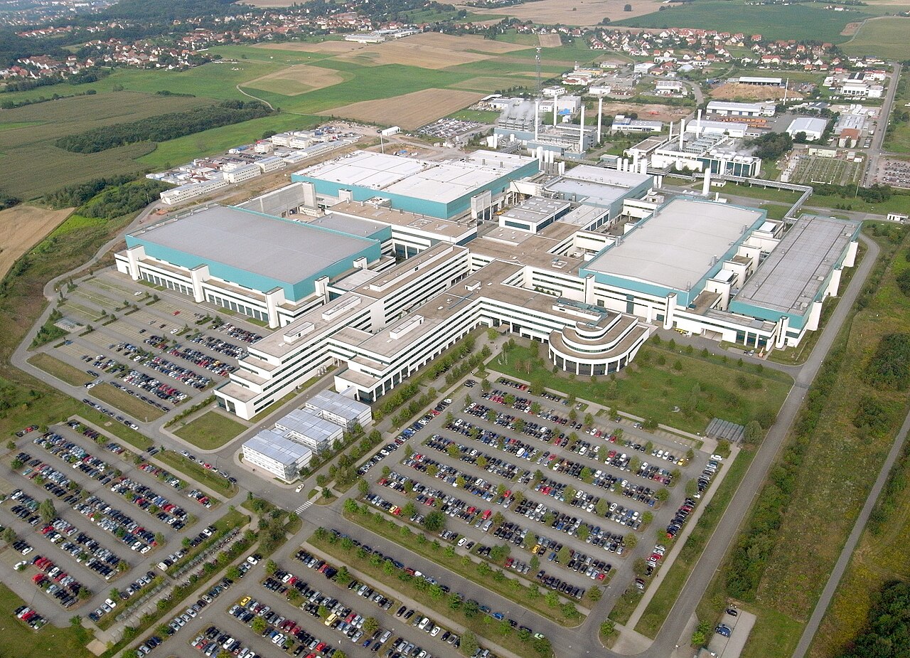
Header image: aerial photograph of the GlobalFoundries campus in Dresden, Germany, by Fensterblick., via Wikimedia Commons, licensed CC BY-SA 3.0. In-body photograph of the Dresden entrance and gatehouse by Albrecht Voss, via Wikimedia Commons, licensed CC BY-SA 4.0. Both photographs are illustrative and do not show the Malta, New York site.