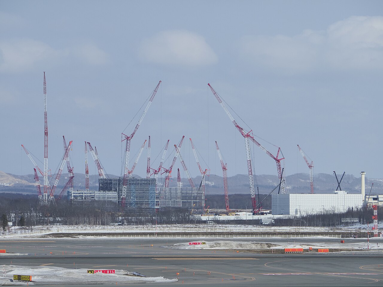
Rapidus, the Japanese state-backed contract chipmaker, has lined up 17 design partners to help prospective customers design chips for its 2nm process, according to reports published on October 5 and 6, 2026. The announcement matters less as a headline number than as a signal about what a new foundry lacks on day one: not just a factory, but the tools, libraries and engineering teams that let a customer turn a chip idea into a manufacturable design. This article covers what was announced, how Rapidus is funded, how its timeline sits against TSMC, Samsung and Intel, and why design partners are central to a foundry that has no customer base yet.
What Rapidus announced: 17 design partners for 2nm
Per Nikkei Asia and Jiji Press coverage, Rapidus will work with 17 companies that help clients design semiconductors, with the aim of winning manufacturing contracts. The group named in reports includes the electronic design automation (EDA) vendors Cadence and Synopsys (both U.S.), Japanese firms Toshiba Information Systems, Dai Nippon Printing (DNP) and Toppan, and design-services companies HCLTech, Infosys, MosChip and Wipro.
IN Electronics reports that the program is called Rapidus CORE, short for Collaborative Open Rapid Ecosystem, and that the partners are labelled Design Solution Associates. They are described as providing engineering resources and acting as a bridge between customers and the foundry. The same report says CORE is meant to cover EDA tool flows, process design kits (PDKs), verified IP blocks, design services and verification, and that Rapidus plans to extend it to semiconductor IP, advanced packaging, interface standards and testing.
One timing detail needs care. A report carried by Mezha says production is planned for the second half of the next fiscal year, while The Register in April described mass production as targeted for the second half of 2027, and Rapidus's own funding releases say "by 2027." Japanese fiscal years begin in April, so a fiscal-year reading would place the second half between October 2027 and March 2028. We could not reconcile these wordings from the sources reviewed, so treat the exact start as a window rather than a date.
Why design partners matter for a new foundry
A foundry sells manufacturing, but a customer buys a path from concept to working silicon. For that path a leading-edge process needs several things to exist before the first order:
- A PDK. The process design kit is the rulebook and model set a designer uses to draw circuits that the fab can build. Without a validated PDK, a chip cannot be signed off.
- EDA tool flows. Synopsys and Cadence tools must be tuned to the process, so synthesis, place-and-route and timing sign-off produce results that match silicon.
- Verified IP. Memory compilers, interface blocks and standard cells that are already proven on the process save customers from redoing basic work.
- Engineering capacity. Many companies that would buy a custom chip lack large internal design teams, so service firms supply the labor.
The Register quotes Stephen DiFranco, Rapidus's partner ecosystem lead, saying the company is seeing more companies that need modest volumes per project. That is the segment where outside design help is most valuable, because a smaller customer cannot absorb the cost of building a full flow alone. In that sense the 17 partners are less a customer list than an on-ramp, and the commercial test is how many become wafer orders.
The most important question for Rapidus is who will actually fill the facility's production capacity.
Analyst quoted in Mezha's report on the 17 partnerships
Funding: how the state backs Rapidus
Rapidus is funded by a mix of equity and government R&D subsidies, and the sources count them differently, so figures should not be added together casually.
On the equity side, a February 27, 2026 release reported 267.6 billion yen raised: 100 billion yen from Japan's Information-Technology Promotion Agency (IPA, under the Ministry of Economy, Trade and Industry) and 167.6 billion yen from 32 private companies, including Canon, Fujitsu, NTT, SoftBank and Sony Group. Together with 7.3 billion yen raised at founding, capital plus legal capital surplus reached 274.95 billion yen. A June 5, 2026 release added 150 billion yen from IPA, bringing the total to 424.95 billion yen.
Rapidus equity capital by source, 2022 to June 2026
Billions of yen, stated capital plus legal capital surplus. Equity only: the larger government R&D subsidies are separate and are not shown here.
Sources: Rapidus press releases of Feb 27, 2026 and Jun 5, 2026 (cumulative total 424.95 billion yen). Hover a bar for values.
On the subsidy side, The Register reported in April 2026 that the ministry approved an additional 631.5 billion yen, putting cumulative R&D assistance at 2.354 trillion yen. Separately, TrendForce reported on November 24, 2025 that the ministry announced another 1 trillion yen for fiscal years 2026 to 2027, with the plan lifting total government backing to 2.9 trillion yen, including in-kind contributions such as state-funded buildings and equipment exchanged for equity. It also reported a government "golden share" with veto rights over matters such as technology partnerships, a profitability target of fiscal 2030 and an IPO in fiscal 2031. The 2.9 trillion and 2.354 trillion figures come from different dates and definitions, which we could not fully reconcile.

IIM-1 in Chitose and the IBM link
Rapidus's first plant, IIM-1, is in Chitose, Hokkaido. Electronics For You reports it became operational in April 2025 with more than 200 tools, including ASML extreme ultraviolet (EUV) lithography equipment, and that on July 18, 2025 Rapidus validated a 2nm gate-all-around (GAA) nanosheet prototype with expected electrical characteristics. The same report describes a single-wafer processing approach, handling wafers individually rather than in batches to allow real-time feedback.
The technology lineage runs through IBM. The Register reports Rapidus partnered with IBM to commercialize the 2nm process IBM developed at its Albany, New York lab, which introduced gate-all-around transistors. Electronics For You adds that Rapidus sent engineers to the U.S. for training and co-develops mass-production techniques with IBM. For customers, this matters because the node is derived from a documented research process, though a research process and a high-yield production process are different things.
How Rapidus compares with TSMC, Samsung and Intel
Rapidus would be the fourth company offering 2nm-class logic, and it is entering as others have already shipped.
2nm-class volume milestones: reported dates vs Rapidus target
Reported milestones for TSMC, Samsung and Intel (past) against Rapidus's stated target window (future). Node names are marketing labels and are not directly comparable.
Sources: TSMC Q4 2025 earnings commentary, TrendForce (Dec 19, 2025), Intel Newsroom, The Register (Apr 14, 2026). Bar widths show the quarter or window reported.
- TSMC. Its Q4 2025 earnings commentary said N2 entered high-volume manufacturing in the quarter with good yield, per a summary of the results. In Q2 2026, N2 was about 3% of wafer revenue, and management described a steep ramp and capacity growth of roughly 70% a year from 2026 to 2028, per the Q2 call transcript. Our earlier coverage of TSMC's Q2 2026 results covers that ramp.
- Samsung. TrendForce reported that Samsung listed the Exynos 2600, built on its SF2 2nm GAA process, as in "mass production" on December 19, 2025, with industry estimates of yields around 60% or higher. Those yield figures are estimates, not Samsung disclosures.
- Intel. Intel said its Core Ultra series 3 (Panther Lake) processors, made on Intel 18A at Fab 52 in Arizona, would go on sale in January 2026.
Node names are marketing labels, so these are milestones on comparable generations rather than equivalent products. The practical point is that Rapidus's target lands roughly 18 months or more after the incumbents' first volume milestones, by which time they will have refined their processes and ecosystems.
AI chip demand: the opening Rapidus is aiming at
The case for a fourth 2nm supplier rests on demand outrunning capacity. As we reported in our analysis of AMD's 2027 supply plan, Taiwanese press reported that Nvidia, AMD and Apple raised 2nm orders at TSMC, and that advanced capacity is increasingly the pacing item for AI hardware. Rapidus CEO Atsuyoshi Koike has argued, per Mezha, that one or two companies are not enough to meet global demand.
 Nvidia
 AMD
AMD Apple
AppleThere is a counterweight. The largest AI buyers book capacity years ahead at the incumbents, while the segments Rapidus describes targeting are smaller-volume, specialized chips. Whether those buyers accept a new supplier depends on yield, schedule reliability and price, none of which is knowable until the line runs at volume.
What to watch next
- The first named customers. Design partners are an on-ramp. Public wafer commitments would be the first evidence that the ecosystem converts.
- PDK maturity. Rapidus said in 2025 that it planned to supply design kits to customers by early 2026. The reports reviewed do not confirm the current PDK version or release status.
- Yield disclosures. None of the sources reviewed gives Rapidus yield figures, which will decide cost per good die.
- Production timing language. Whether the start is described in calendar or fiscal terms will clarify the window.
For teams following chip supply as an input to model and compute planning, the practical lesson is to track supplier diversity rather than any single announcement.
Sources:
- Japan's Rapidus to help 17 companies design chips for clients | Nikkei Asia
- Japan's Rapidus Teams with 17 Firms on Chip Design Support | Jiji Press via Nippon.com
- Rapidus builds CORE around 2nm design ecosystem | IN Electronics
- Japan's Rapidus Partners with 17 Firms as It Seeks Customers for 2nm Chips | Mezha
- Rapidus Secures 267.6 Billion Yen in Funding | Rapidus
- Rapidus Completes 150 Billion Yen Funding Round from Japan Government | Rapidus
- Japan's semiconductor industry comeback and Rapidus | The Register
- Japan reportedly adding 1 trillion yen in Rapidus support | TrendForce
- Japan's Rapidus enters elite semiconductor league with 2nm prototype | Electronics For You
- TSMC Q4 2025 earnings summary | VectorShift
- TSMC Q2 2026 earnings call transcript | Investing.com
- Samsung Exynos 2600 production status | TrendForce
- Introducing Panther Lake: By the Numbers | Intel Newsroom
Image credits
Header image: Rapidus factory under construction in Chitose, seen from New Chitose Airport, photographed in March 2024 (a file photo of construction, not of the finished or operating plant), by どういたしまして via Wikimedia Commons, licensed under CC BY-SA 4.0. In-body photograph of Tetsuro Higashi and Sanae Takaichi, Cabinet Public Relations Office of the Cabinet Secretariat via Wikimedia Commons, licensed under CC BY 4.0.